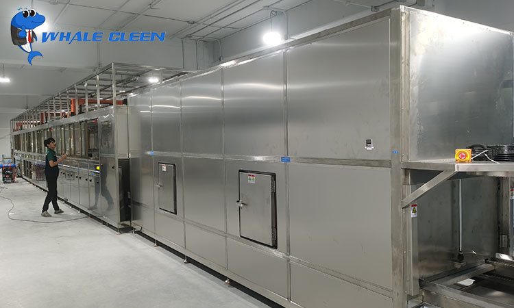
In the ever-evolving world of semiconductor manufacturing, maintaining ultra-clean environments is critical. The microscopic scale at which semiconductor devices operate means that even the smallest contaminant can render a component defective, causing failures in electronic devices. Traditional cleaning methods have struggled to meet the increasingly stringent requirements of modern semiconductor fabrication. However, ultrasonic cleaning machines have emerged as a powerful solution, heralding a new era of cleanliness in the industry.
Ultrasonic cleaning technology utilizes high-frequency sound waves to create cavitation bubbles in a liquid cleaning solution. These bubbles collapse violently, generating localized high temperatures and pressures. This cavitation process effectively dislodges contaminants from surfaces, including particles, residues, and films, without damaging the delicate components being cleaned.
The core of ultrasonic cleaning lies in the transducers, which convert electrical energy into ultrasonic waves. These waves, typically operating in the range of 20 kHz to 400 kHz, create rapid pressure changes in the cleaning liquid. The effectiveness of the cleaning process can be fine-tuned by adjusting parameters such as frequency, power, temperature, and the composition of the cleaning solution. The versatility of this technology makes it ideal for various applications in semiconductor manufacturing.
As semiconductor devices become smaller and more complex, the demand for ultra-pure environments intensifies. Contaminants such as particles, organic residues, and metal ions can adversely affect the performance and yield of semiconductor wafers. Traditional cleaning methods, such as chemical baths and mechanical scrubbing, often fall short in achieving the required level of cleanliness, especially for structures on the nanometer scale.
Ultrasonic cleaning machines provide a more effective solution by reaching into minute crevices and intricate geometries that are otherwise difficult to clean with conventional methods. This is particularly important in semiconductor manufacturing, where wafers are processed through numerous steps, each introducing potential contamination risks. By integrating ultrasonic cleaning at various stages, manufacturers can significantly reduce defects and improve overall yield.
Enhanced Cleaning Efficiency:Ultrasonic cleaning machines offer superior cleaning efficiency by removing contaminants at a microscopic level. The cavitation effect generated by the ultrasonic waves reaches every nook and cranny of the component being cleaned, ensuring thorough decontamination without the need for harsh chemicals or manual scrubbing.
Reduced Use of Chemicals:Traditional semiconductor cleaning methods often rely heavily on chemicals, which can be harmful to both the environment and personnel. Ultrasonic cleaning reduces the need for aggressive chemicals, making it a greener and safer alternative. The process typically uses water-based or mild solvent solutions, minimizing the environmental footprint of semiconductor manufacturing.
Minimization of Physical Damage:Sensitive semiconductor components, such as wafers and microchips, can be easily damaged by physical contact during cleaning. Ultrasonic cleaning is a non-contact process, which eliminates the risk of scratching or abrading delicate surfaces. This is crucial in preserving the integrity of components throughout the manufacturing process.
Versatility and Adaptability:Ultrasonic cleaning machines can be customized to suit various cleaning requirements in semiconductor manufacturing. Parameters like frequency, power, and temperature can be adjusted to optimize the cleaning process for different types of contaminants and component geometries. This adaptability ensures that ultrasonic cleaning can be effectively integrated into multiple stages of the production process.
Improved Yield and Reliability:By achieving higher levels of cleanliness, ultrasonic cleaning helps reduce defects and contamination-induced failures in semiconductor devices. This leads to improved yield rates and greater reliability of the final products, which is essential in meeting the high standards of modern electronics.
Ultrasonic cleaning machines find applications in various stages of semiconductor manufacturing, from wafer production to final assembly. Some of the key applications include:
Wafer Cleaning: During the wafer fabrication process, multiple layers of materials are deposited, patterned, and etched. Ultrasonic cleaning is used to remove particulate matter, organic residues, and process-induced contaminants, ensuring that each wafer surface is pristine before the next processing step.
Photomask Cleaning: Photomasks are critical tools used in photolithography, where patterns are transferred onto the wafer surface. Any contamination on the photomask can result in defective patterns, leading to faulty devices. Ultrasonic cleaning ensures that photomasks are free from contaminants, preserving pattern fidelity.
Component Cleaning: Beyond wafers, ultrasonic cleaning is also used to clean various components such as quartz, ceramic, and metal parts used in semiconductor equipment. These components require regular cleaning to maintain optimal performance and prevent cross-contamination during wafer processing.
Final Device Cleaning: Before final packaging, semiconductor devices undergo ultrasonic cleaning to remove any remaining contaminants. This step is crucial in ensuring the reliability and performance of the devices in their intended applications.
The continuous advancement in semiconductor technology necessitates the evolution of cleaning processes. Ultrasonic cleaning machines are evolving to meet these demands, with innovations such as megasonic cleaning (utilizing frequencies above 1 MHz) being developed for even finer control over the cleaning process. Megasonic cleaning, with its smaller cavitation bubbles and reduced intensity, is particularly effective for cleaning delicate features on wafers and other semiconductor components.
Furthermore, the integration of ultrasonic cleaning systems with automated robotic handling and in-line monitoring technologies is becoming increasingly common. These advancements enable real-time process control, reducing cycle times and improving overall efficiency in semiconductor fabrication.
Ultrasonic cleaning machines have established themselves as indispensable tools in semiconductor manufacturing, providing a level of cleanliness that is critical for the production of high-performance, reliable electronic devices. Their ability to effectively remove contaminants without damaging delicate components, reduce chemical usage, and improve yield rates positions them as a cornerstone of advanced semiconductor fabrication processes.
As the semiconductor industry continues to push the boundaries of miniaturization and complexity, the role of ultrasonic cleaning technology will only grow in importance, driving further innovations and setting new standards for cleanliness in the manufacturing process.
By utilizing ultrasonic cleaning technology, semiconductor manufacturers are better equipped to meet the ever-increasing demands for higher precision and reliability in microelectronics. As a result, ultrasonic cleaning machines are not just enhancing current manufacturing capabilities but are also paving the way for future advancements in the semiconductor industry.

Related Issues not found
Please contact @269986972 to initialize the comment